When it comes to PCB (Printed Circuit Board) manufacturing for consumer electronics, even the smallest mistake can lead to major product failures, costly redesigns, or delayed launches. Whether you’re designing smart gadgets, wearable devices, or home automation systems, ensuring your PCB is error-free is crucial for both performance and customer satisfaction.
In this article, we’ll walk through common PCB mistakes and how to avoid them—helping you save time, reduce costs, and deliver reliable products to market.
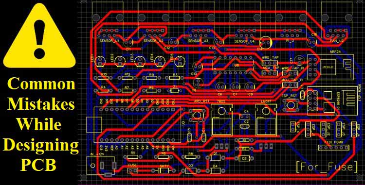
1. Poor Component Placement
One of the most frequent mistakes in PCB making is poor component layout. Improper placement can lead to signal interference, thermal issues, and difficulties during assembly.
How to avoid it:
-
Place high-speed components close to each other to minimize trace length.
-
Keep analog and digital sections separate.
-
Place decoupling capacitors near power pins.
-
Always consider heat-sensitive components and place them away from heat-generating parts.
2. Inadequate Trace Widths
Undersized traces can cause overheating and even circuit failure under high current.
Solution:
-
Use trace width calculators based on the expected current load.
-
Follow IPC-2221 standards for trace design.
-
Factor in both internal and external layers when determining width.
3. Ignoring Design for Manufacturability (DFM)
Designs that look great on-screen may be difficult or costly to manufacture in reality.
Fix:
-
Collaborate with your PCB manufacturer early in the design process.
-
Use standard hole sizes and spacing to avoid custom fabrication.
-
Avoid overly tight tolerances unless absolutely necessary.
4. Skipping Thermal Management
Many consumer electronics are compact and generate significant heat. Failing to plan for thermal management can reduce the lifespan of your product.
Avoid this by:
-
Including thermal vias under power components.
-
Using copper pours to dissipate heat.
-
Considering the airflow inside the final enclosure.
5. Overlooking Grounding and EMI Issues
Improper grounding and poor EMI (Electromagnetic Interference) control can cause erratic behavior and signal integrity problems.
Tips to get it right:
-
Use a solid ground plane.
-
Keep return paths short and direct.
-
Shield high-speed traces and separate noisy and sensitive signals.
6. Not Running Design Rule Checks (DRC)
Skipping DRCs or running them too late in the process can allow critical design flaws to slip through.
Best practice:
-
Run DRCs frequently during the design process.
-
Use manufacturer-specific DRC settings for more accurate results.
7. Underestimating Testing and Prototyping
Rushing into production without thorough testing often leads to expensive recalls or customer dissatisfaction.
How to avoid:
-
Always prototype before mass production.
-
Perform functional testing, in-circuit testing (ICT), and environmental stress testing.
-
Work with a PCB assembly partner that offers in-house testing services.
Final Thoughts
Avoiding these common PCB mistakes is essential to creating high-quality, durable consumer electronics. By emphasizing smart layout, thermal design, manufacturability, and proper testing, you set your product up for success in a competitive market.
Whether you’re a startup building the next wearable tech or an established brand developing IoT devices, partnering with an experienced PCB manufacturer can be the key to turning your designs into reliable products.